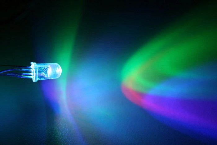
Osioptoelectronics A Comprehensive Overview
Optoelectronics is a rapidly evolving field at the intersection of optics and electronics, enabling the manipulation and transmission of light for various applications. From its historical roots in semiconductor physics to its current role in high-speed communication, osioptoelectronics has become an essential technology. This overview explores the fundamental principles, materials, devices, applications, and challenges within this field, highlighting its significance and potential.
The field encompasses a wide range of materials and devices, each with unique properties and functionalities. Key components of osioptoelectronic systems, such as optical fibers and lasers, will be examined. Further, we will delve into the diverse applications, from optical communication to sensing and energy conversion. The potential impact of osioptoelectronics on technological advancements will be a key discussion point, along with the challenges and future directions.
Introduction to Osioptoelectronics
Source: maker.pro
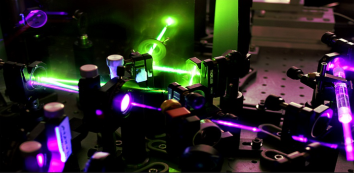
Osioptoelectronics, a rapidly evolving field, integrates optical and electronic technologies to create devices with unique capabilities. It leverages the properties of light and semiconductors to process information and transmit signals with unprecedented speed and efficiency. This interdisciplinary approach allows for the development of compact, high-performance systems, pushing the boundaries of current technology.
Definition of Osioptoelectronics
Osioptoelectronics encompasses the design, fabrication, and application of electronic devices that utilize light to perform various functions. This includes the generation, manipulation, and detection of light signals for information processing and transmission. It bridges the gap between electronics and photonics, enabling new functionalities in diverse fields.
Historical Context
The historical development of osioptoelectronics is intrinsically linked to advancements in both optics and electronics. Early work on semiconductor lasers and photodiodes paved the way for integrated optical circuits and optical communication systems. The invention of the laser in the mid-20th century marked a crucial turning point, opening doors to applications ranging from optical storage to high-speed data transmission. Continuous research and development have led to the emergence of sophisticated osioptoelectronic devices and systems, significantly enhancing the performance of various technologies.
Fundamental Principles
Osioptoelectronics relies on the fundamental principles of quantum mechanics, semiconductor physics, and electromagnetism. The interaction between light and matter is central to its operation. Key concepts include the generation of light through stimulated emission (e.g., lasers), the manipulation of light through optical waveguides, and the detection of light using photodiodes. Understanding these principles is crucial for the design and optimization of osioptoelectronic devices.
Key Applications
Optoelectronics finds applications across diverse fields. In telecommunications, it enables high-speed data transmission through optical fibers. In computing, it facilitates faster data processing and enhanced storage capacities. Furthermore, osioptoelectronic devices are utilized in medical imaging, sensing, and actuation. This widespread adoption demonstrates the transformative potential of osioptoelectronics across various sectors.
Current Research Trends
Current research in osioptoelectronics focuses on developing more efficient and compact devices. Researchers are exploring novel materials with improved optical properties and enhanced functionalities. Further investigation into integrated photonic circuits aims to achieve greater integration density and reduce signal loss. These advancements hold the key to creating more powerful and energy-efficient osioptoelectronic systems.
Future Directions
The future of osioptoelectronics is promising, with anticipated advancements in several areas. One area of interest is the development of ultra-fast optical communication systems for next-generation networks. Furthermore, researchers are investigating the potential of osioptoelectronics in quantum computing and sensing. The integration of osioptoelectronic devices with other emerging technologies will likely lead to significant breakthroughs in the coming years.
Key Components of a Typical Osioptoelectronic System
| Component | Description | Function |
|---|---|---|
| Light Source (e.g., Laser Diode) | A device that emits light. | Generates the optical signal for transmission or processing. |
| Optical Components (e.g., Lenses, Mirrors, Waveguides) | Devices that manipulate and guide light. | Focus, direct, and shape the light beam for efficient signal transmission. |
| Photodetectors (e.g., Photodiodes) | Devices that convert light into electrical signals. | Detect and convert the optical signal back into an electrical signal. |
| Electronic Circuits | Processing units that handle the electrical signals. | Process, amplify, and modulate the electrical signals. |
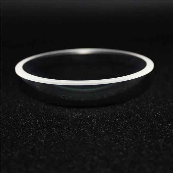
Materials and Devices

Source: mordorintelligence.com
Optoelectronic devices leverage the unique properties of various materials to manipulate light and electrical signals. This crucial aspect encompasses the selection of materials, their fabrication into functional devices, and the resulting performance characteristics. Understanding these facets is fundamental to designing efficient and effective osioptoelectronic systems.
Key Semiconductor Materials
Semiconductor materials are the cornerstone of optoelectronic devices. Their ability to modulate light and electrical signals makes them essential. The specific material choice hinges on the desired application and performance parameters. Different semiconductors exhibit varying bandgaps, conductivities, and optical properties, leading to diverse functionalities.
Material Properties and Characteristics
A critical factor in material selection is the bandgap energy. This determines the energy required to excite electrons from the valence band to the conduction band, influencing the device’s operating wavelength. High bandgap materials, like gallium arsenide (GaAs), are suited for shorter wavelengths, while lower bandgap materials, such as indium gallium arsenide phosphide (InGaAsP), are suitable for longer wavelengths. Material conductivity plays a significant role in device performance, impacting the speed and efficiency of charge carrier movement. Optical properties, including absorption and emission characteristics, are crucial for light manipulation.
Material Comparison for Applications
Silicon (Si) is widely used in photovoltaic cells due to its abundance and cost-effectiveness. However, its indirect bandgap limits its efficiency in optoelectronic applications compared to direct bandgap materials. Gallium arsenide (GaAs) and its alloys are preferred for high-speed optoelectronic devices like lasers and photodetectors due to their high electron mobility and direct bandgap. For applications requiring specific wavelengths, such as in optical communication systems, materials like InGaAsP are crucial for their tunability. Choosing the right material for a particular application depends on a trade-off between cost, performance, and available technology.
Fabrication Processes
Optoelectronic devices often involve sophisticated fabrication processes, including crystal growth, doping, and lithography. Crystal growth techniques like the Czochralski and Bridgman methods yield high-quality semiconductor crystals. Doping introduces controlled impurities to alter the electrical properties of the material, and lithography patterns intricate features for device functionality. These processes require precise control over temperature, pressure, and doping concentrations to achieve the desired material properties.
Advantages and Disadvantages of Fabrication Techniques
Different fabrication techniques offer unique advantages and disadvantages. Czochralski growth, for instance, allows for large-scale production of high-quality crystals, but it can be expensive. Molecular beam epitaxy (MBE) provides precise control over layer thickness and composition, but it often has lower throughput compared to other techniques. The selection of fabrication methods often involves a trade-off between cost, precision, and production rate.
Semiconductor Material Properties Table
| Material | Bandgap (eV) | Conductivity (S/cm) | Typical Application |
|---|---|---|---|
| Silicon (Si) | 1.12 | Low | Photovoltaics |
| Gallium Arsenide (GaAs) | 1.42 | High | High-speed lasers, photodetectors |
| Indium Gallium Arsenide Phosphide (InGaAsP) | 0.7 – 1.6 | Moderate | Optical communication |
| Cadmium Telluride (CdTe) | 1.44 | Moderate | Solar cells |
This table highlights the key properties of common semiconductor materials used in osioptoelectronics. Note that these values are approximate and can vary based on specific doping and processing conditions.
Optical Properties and Performance
Optoelectronic devices rely heavily on their optical properties for functionality. These properties dictate how light interacts with the device, influencing its performance in applications ranging from optical communication to sensing. Understanding these properties and the factors affecting them is crucial for optimizing device performance and achieving desired outcomes.
Optical Properties of Osioptoelectronic Devices
Optoelectronic devices exhibit a range of optical properties crucial to their operation. These properties include absorption, emission, reflection, and transmission of light. The interaction of light with the material’s structure determines the device’s response to incident light. For instance, the bandgap energy of the semiconductor material dictates the wavelengths of light that can be absorbed or emitted, influencing the device’s operating spectral range.
Factors Affecting Osioptoelectronic Device Performance
Several factors influence the performance of osioptoelectronic devices. These factors include material quality, device structure, fabrication process, and environmental conditions. Material impurities, structural defects, and variations in doping concentration can all lead to performance degradation. Precise control over these factors is essential for achieving optimal device performance. Environmental conditions, such as temperature and humidity, can also affect the device’s optical properties, potentially altering its performance characteristics.
Examples of Optical Property Influence on Device Performance
The bandgap energy of a semiconductor material directly affects the wavelengths of light it can absorb or emit. A smaller bandgap allows for absorption and emission of longer wavelengths, shifting the device’s operating range toward the infrared spectrum. For example, in solar cells, a material with a bandgap matched to the solar spectrum maximizes light absorption, leading to higher efficiency. Similarly, in light-emitting diodes (LEDs), the bandgap determines the color of light emitted. The choice of material dictates the wavelength, influencing the application of the LED, whether it’s for displays or illumination.
Methods for Measuring Optical Performance
Several methods are used to measure the optical performance of osioptoelectronic devices. These methods include spectrophotometry, which measures the absorption and transmission characteristics of a material over a range of wavelengths. Photoluminescence (PL) spectroscopy measures the emitted light intensity and wavelength from a material when stimulated by light. These measurements provide crucial data on the material’s optical properties and aid in the design and optimization of osioptoelectronic devices. Furthermore, external quantum efficiency (EQE) measurements determine the efficiency of converting photons into electrons, a critical metric for photodetectors.
Comparison of Optical Performance in Different Osioptoelectronic Devices
| Device Type | Bandwidth (THz) | Efficiency (%) |
|---|---|---|
| Photodetector (Silicon) | 10-100 | 50-80 |
| Laser Diode (InGaAsP) | 1-10 | 50-70 |
| LLight-EmittingDiode (LED) (GaN) | 0.1-1 | 10-50 |
Note: Values are approximate and can vary significantly based on specific device design and material properties.
Applications and Systems
Optoelectronics, encompassing the integration of optics and electronics, has revolutionized various technological domains. Its unique capabilities enable efficient signal processing, data transmission, and sensing, leading to innovations in communication, imaging, and energy conversion. This section delves into the diverse applications and systems where osioptoelectronics play a pivotal role.
Diverse Applications
Optoelectronics find applications in a wide array of fields. From high-speed data transmission in optical communication networks to precise measurements in sensors, its versatility is remarkable. These applications rely on the unique properties of materials and devices, allowing for efficient manipulation and control of light.
Optical Communication Systems
Optoelectronics are integral to modern optical communication systems. The ability to encode information onto light waves and transmit it over long distances with minimal signal degradation makes it superior to traditional electrical communication methods. Laser diodes, photodiodes, and optical fibers are key components enabling high-bandwidth and long-haul communication systems. Optical communication systems are crucial for global internet connectivity, telecommunications, and data centers.
Sensing and Imaging
Optoelectronics are increasingly important in sensing and imaging applications. Photonic sensors, which use light interaction with materials, enable highly sensitive detection of physical parameters like temperature, pressure, and chemical composition. Furthermore, advancements in imaging technologies utilize light to create detailed images with high resolution, such as in medical imaging and industrial inspection. This allows for real-time monitoring and analysis of diverse phenomena.
Energy Harvesting and Conversion
Optoelectronics are actively explored for energy harvesting and conversion. Solar cells and photodetectors are examples of devices converting solar energy into electrical energy. These advancements are essential for sustainable energy solutions, particularly in remote areas or locations with limited access to traditional power grids. Furthermore, they enable advancements in areas like self-powered sensors and portable electronic devices.
Applications and Components Table
| Application | System Component | Functionality |
|---|---|---|
| Optical Communication | Laser Diodes, Optical Fibers, Photodiodes | Transmit and receive optical signals over long distances with high bandwidth. |
| Medical Imaging | Optical Fibers, Photodetectors, Light Sources | Create high-resolution images of internal body structures using light interaction. |
| Environmental Monitoring | Photonic Sensors, Optical Detectors | Detect and measure environmental parameters like air quality, water purity, and pollution levels. |
| Solar Energy Conversion | Solar Cells, Photovoltaic Devices | Convert solar energy into usable electrical energy. |
| Industrial Sensing | Fiber Optic Sensors, Light Detection Devices | Measure physical parameters in industrial processes for quality control and safety. |
Challenges and Future Prospects: Osioptoelectronics
Osioptoelectronics, while holding immense promise, faces several hurdles that need careful consideration for its continued advancement. These challenges, coupled with emerging research directions, will shape the future trajectory of this field, influencing technological progress across diverse sectors. Overcoming these obstacles is crucial to realizing the full potential of osioptoelectronics.
Current Challenges, Osioptoelectronics
Several critical challenges hinder the widespread adoption and optimization of osioptoelectronic systems. These include the need for improved material properties, reduced fabrication costs, enhanced device performance, and integration into complex systems. Furthermore, achieving stable and reliable operation in diverse environments presents significant obstacles.
Potential Solutions
Addressing the aforementioned challenges requires a multi-pronged approach. Advancements in material science, particularly in developing novel materials with tailored optical and electronic properties, are crucial. Simultaneously, innovative fabrication techniques and cost-effective manufacturing processes are essential. Improved device designs and integration strategies will enable the creation of more compact and efficient systems.
Emerging Research Areas
Emerging research areas in osioptoelectronics include the development of novel materials, such as those with enhanced light emission, absorption, or manipulation capabilities. Additionally, research into more efficient energy transfer mechanisms and advanced device architectures is actively pursued. Another key area involves the development of integrated systems that combine various osioptoelectronic components into compact, robust, and functional modules.
Future Prospects
The future of osioptoelectronics is bright, promising significant advancements across numerous technological domains. For example, advancements in high-speed optical communication systems, energy-efficient sensors, and miniaturized optical devices are anticipated. The potential for widespread adoption in diverse sectors, including telecommunications, medical imaging, and environmental monitoring, is substantial.
Impact on Technological Advancements
Osioptoelectronics is poised to significantly impact technological advancements by enabling faster data transmission rates, more sensitive sensing capabilities, and miniaturized devices. The potential for developing novel applications in areas like quantum computing and advanced imaging techniques is also noteworthy. For example, the development of more efficient solar cells based on osioptoelectronic principles holds great promise.
Areas for Further Research
Further research is required in several areas to address the challenges and unlock the full potential of osioptoelectronics. This includes the development of cost-effective and scalable manufacturing processes for osioptoelectronic devices, the exploration of novel materials with enhanced optical and electronic properties, and the optimization of device architectures for improved performance and reliability.
Table of Major Challenges and Potential Solutions
| Challenge | Potential Solution | Impact |
|---|---|---|
| Limited material properties (e.g., low efficiency, instability) | Development of novel materials with enhanced optical and electronic properties, tailored for specific applications. | Improved device performance, wider range of applications, and reduced energy consumption. |
| High fabrication costs | Innovative, cost-effective fabrication techniques and manufacturing processes. | Wider accessibility, increased market adoption, driving wider commercialization. |
| Complex system integration | Modular design principles, standardized interfaces, and improved integration strategies. | Enhanced system performance, reduced complexity in device assembly, and increased efficiency. |
| Environmental instability | Robust device designs and packaging techniques, materials with enhanced stability in various conditions. | Reliable performance in harsh environments, enabling operation in diverse settings. |
Illustrative Examples
Source: slidesharecdn.com
Osioptoelectronic devices represent a diverse array of technologies, each with unique functionalities and applications. Understanding specific examples is crucial for appreciating the versatility and impact of this field. These examples showcase the integration of optical and electronic components to achieve sophisticated functionalities, spanning diverse sectors.
Photodiodes in Optical Communication Systems
Photodiodes are fundamental components in optical communication systems. They convert incident light into an electrical current, enabling the detection and processing of optical signals. This conversion is a cornerstone of optical fiber communication, a vital technology for transmitting data over long distances.
- PIN Photodiodes: These devices utilize a p-n-p junction structure, featuring a wider intrinsic (i) region. This structure offers improved sensitivity and response speed compared to other photodiode types, especially in high-speed data transmission. The wider depletion region enhances the collection of photogenerated carriers.
- Avalanche Photodiodes (APDs): APDs are designed to amplify the photocurrent through an avalanche multiplication effect. This amplification increases the sensitivity of the device, making them suitable for low-light level applications. The multiplication process, however, can also introduce noise.
Laser Diodes in Optical Data Storage
Laser diodes are crucial components in optical data storage systems. Their ability to generate coherent light precisely enables the precise encoding and retrieval of information on optical media.
- Operation Principle: Laser diodes operate on the principle of stimulated emission, where photons emitted by a stimulated atom cause further atoms to emit photons of the same wavelength. This process creates a coherent beam of light with a very specific wavelength. The light emitted by the laser diode is focused and modulated to write or read data onto the storage medium.
- Advantages: Laser diodes offer high-speed data transfer capabilities, high storage capacity, and low power consumption, making them indispensable in modern optical data storage systems. Their compact size also makes them highly suitable for integration into portable devices.
Light-Emitting Diodes (LEDs) in Medical Imaging
Light-emitting diodes (LEDs) are ubiquitous in various applications. Their use in medical imaging is a prime example of their versatile capabilities. LEDs can be used as a light source in various medical imaging techniques.
- Structure: LEDs are semiconductor devices that emit light when an electric current passes through them. The emitted light’s color and intensity are controlled by the semiconductor material used in the device’s construction. Different materials generate different wavelengths of light.
- Applications: In medical imaging, LEDs are often used in endoscopic imaging systems. Their ability to emit precisely targeted light beams allows for detailed visualization of internal structures. This allows medical professionals to perform minimally invasive procedures and diagnose conditions more effectively.
Summary
In conclusion, osioptoelectronics offers a powerful platform for innovation across numerous technological domains. Its ability to manipulate light has led to breakthroughs in communication, sensing, and energy. While challenges remain, ongoing research and development promise continued advancements in osioptoelectronic systems. The field’s potential for future impact is significant, making it a compelling area for continued exploration and development.